The HF transceiver I couldn't finish

I’m slowly thinking about getting back into amateur radio, so I started digging out old projects. I thought, why not publish my struggles with radio-frequency design on my website? There is some value in showing failed projects, after all.
Introduction
At the beginning of my education in liceum, I was rapidly becoming interested in the shortwaves. A year earlier, I had discovered the ham radio club SP2KPD in my hometown and met many helpful hams there. Since electronics and tinkering had always been alluring to me, I never considered simply buying a factory-made transceiver. What I wanted instead was to build a general-coverage receiver, or even a transceiver, myself — so that my creation would be truly mine and I would have complete control over how it worked. That goal proved to be foolish: the scope of the project overwhelmed me.
I oscillated (pun intended) between a classic 0–30 MHz receiver with a traditional quartz filter, an SDR with a Tayloe mixer, and a full-fledged heterodyne transceiver. None of these attempts were fully successful; nonetheless, I think I learned a lot in the process before abandoning them. Shortly afterward, I moved to Poznań to begin my university studies.
It took me over sixteen years to finally return to radio. A lot of things have changed in the meantime. Access to literature and tutorials is now superb. Tremendously useful tools like NanoVNA are available cheaply on AliExpress, and a wealth of RF modules is available as well. LLMs can answer the majority of my design questions.
Before starting fresh again, I unshelved my old schematics and photos and pieced them together as a memorial to my teenage fascination. The majority of the photos were taken before 2010 and were intended not for publication, but for my own documentation. Admittedly, they are of low quality. A lot of information has been lost (such as firmware), because I did not keep proper notes at the time.
I also realized that no other project on this website, except Octoglow, has a similar level of complexity to the transceiver project. Unfortunately, adult responsibilities have limited the scale of my endeavors.
First attempt at 9 MHz heterodyne receiver
At the beginning, I wasn’t thinking about transmitting or becoming a licensed operator, so I focused on the receiving side. Receiving also allowed for smaller antennas; I could get away with a random wire.
After some encouragement and receiving some electronic components from members of the SP2KPD club, my plan settled on a classic heterodyne receiver with a 9 MHz crystal filter, a double-balanced diode mixer in the front end, and an intermediate-frequency amplifier built with double-gate MOSFETs. This resulted in several modules, each described below.
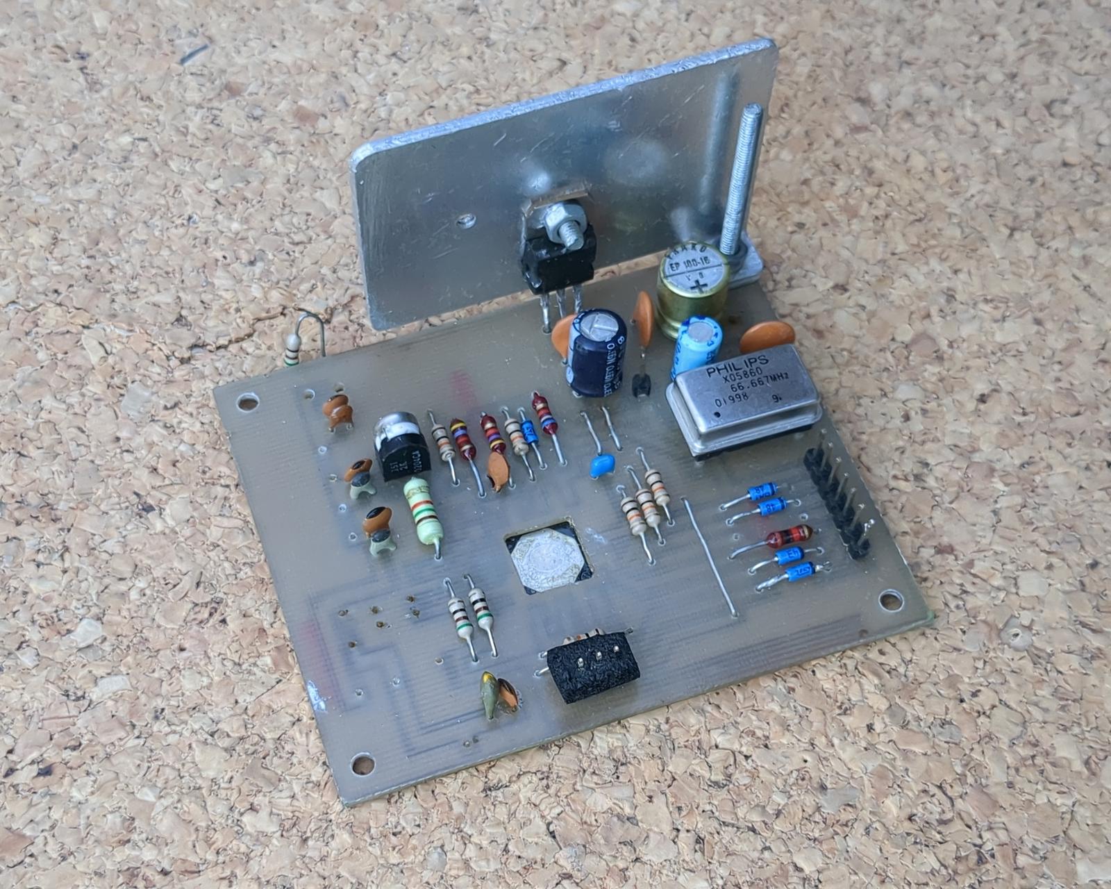
The VFO based on AD9852 DDS
I think I first started entertaining the idea in 2007. I realized that, in order to play with radio frequencies, I needed some measuring equipment. Fortunately, I already owned a 100 MHz four-channel analog oscilloscope at the time, but apart from that I didn’t have much electronics equipment (except mountains of scrap electronics to extract components from, of course). To fill this pressing need, I decided to build a signal generator that would serve not only as a VFO in the finished transceiver, but also as a device for testing other receiver modules.
A classic capacitor-tuned generator wouldn’t provide a precise frequency readout. Moreover, building a proper LC VFO is an art in itself — I knew beforehand that any attempt I made would result in a wobbly, unstable oscillator.
Instead, I opted for a more modern approach and jumped straight into direct digital synthesis after stumbling upon a fairly popular design by SP3SWJ (formerly SP2SWJ), leveraging the AD9851 chip from Analog Devices. I was somewhat concerned about phase noise, but I realized that many hams had already been successfully using DDS-based synthesizers in their transceivers, so it was unlikely to be a problem for a beginner like me.
In retrospect, I should have simply replicated SP3SWJ’s synthesizer boards and assembled them. That would have solved the VFO problem before I moved on to anything else. The LCD and front panel would have been a bonus. But, being myself, I designed my own board instead.
This was my second or so home-made PCB. Previously, I had built all my circuits exclusively on universal PCBs. This was a major step forward in my electronics hobby. I learned CadSoft Eagle in the process, a commercial software package that was popular at the time. Nowadays, I use KiCad for the same purpose.
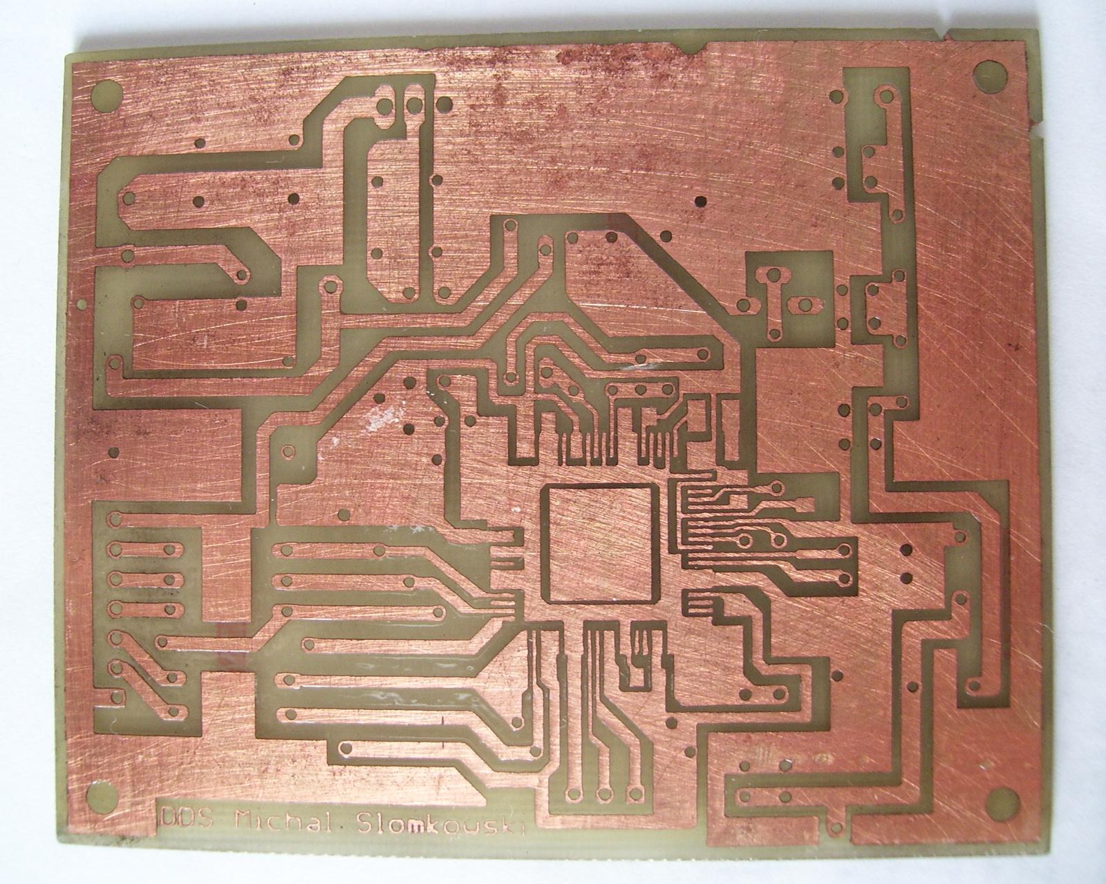
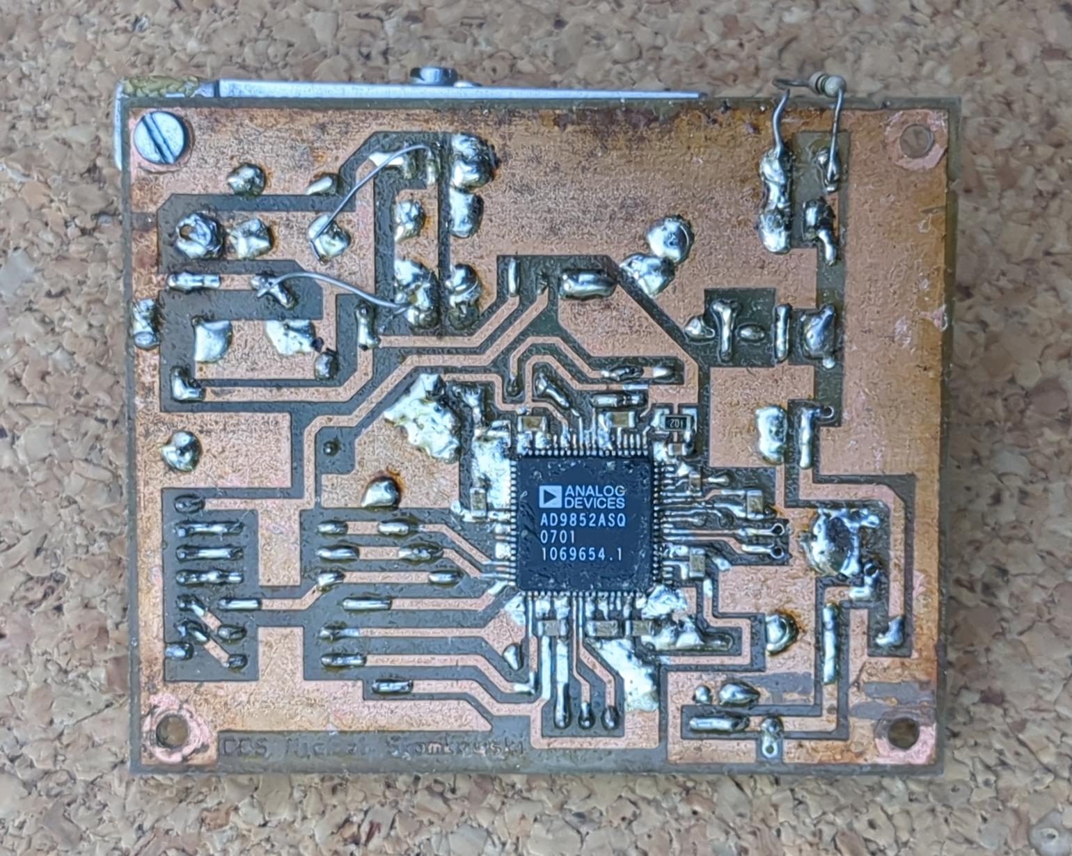
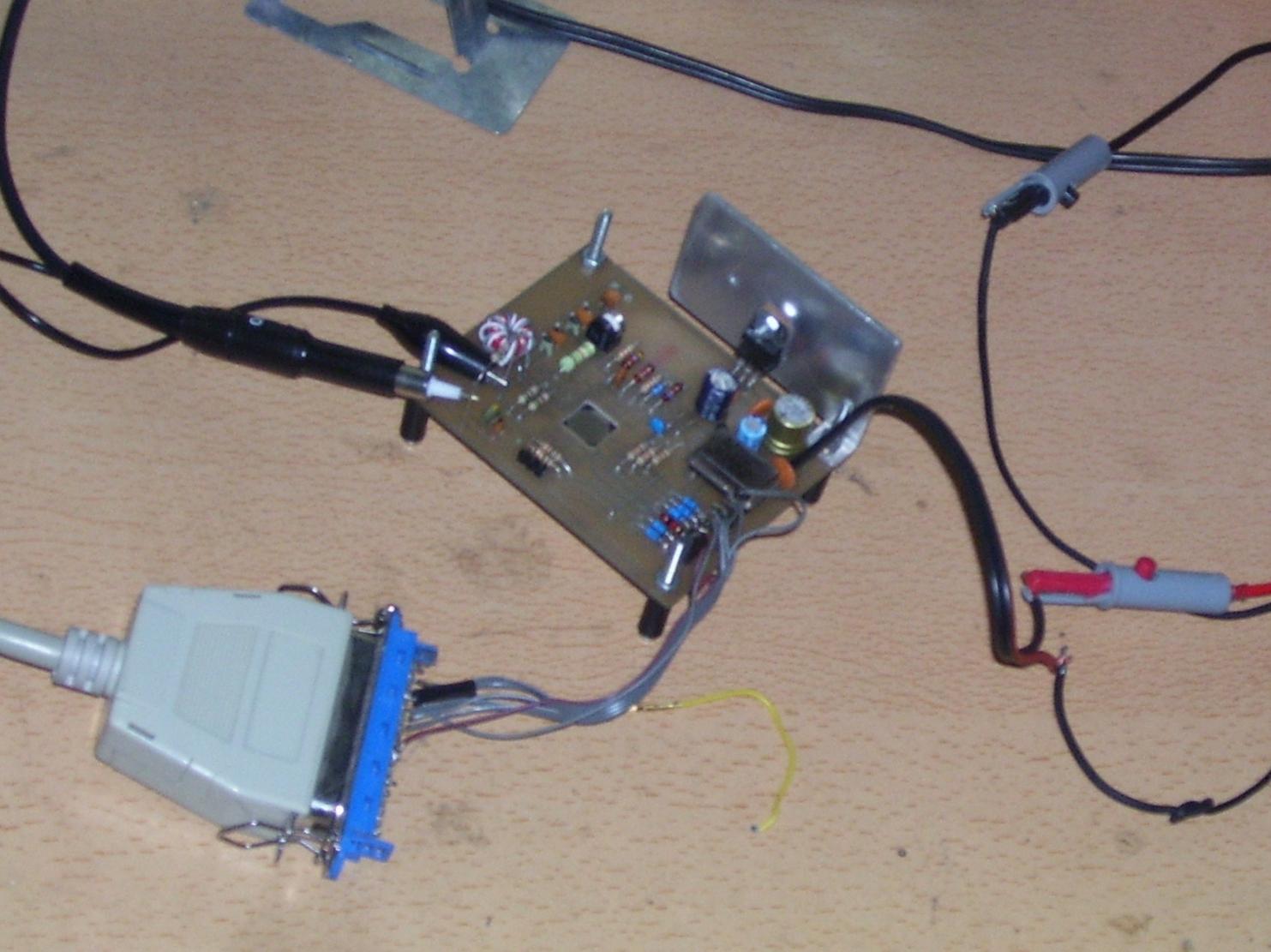
My synthesizer implementation is based on the AD9852 chip. The schematic was copied almost 1:1 from a website from the early 2000s, fortunately mirrored here. The board has six control lines. It was intended to be controlled by an AVR microcontroller, but it can also be connected to a computer via a parallel port. Moreover, there is a small Delphi program for controlling it, written by the author of the aforementioned website.

The connections for the control via LPT:
| AD9852’s pin name | LPT pin number |
|---|---|
MASTER_RESET |
2 |
SCB |
3 |
IO_RESET |
4 |
SCLK |
5 |
SDIO |
6 |
I/O UD |
7 |
The DDS is clocked by a 66.667 MHz crystal oscillator. To make it easy to swap the oscillator for another one, I placed it in a DIP-14 socket. The clock
signal is internally multiplied by a PLL, allowing the DDS output frequency to comfortably reach 39 MHz without
significant degradation from an ideal sine wave. A VFO range of 9 to 39 MHz allows coverage of the entire HF spectrum (0–30 MHz) when using 9 MHz IF
frequency. The AD9852 runs hot, so I cut a hole in the PCB and glued a heat sink directly to the chip. The output is filtered by a
low-pass filter consisting of C8-C11 and L4-L6. L1/L2/L3 form a
wideband transformer that I wound myself on a ferrite core, although I unfortunately no longer have any details.
The AD9852 chip is an SMD component with a lead pitch of 0.6 mm. I was somewhat cautious when soldering it, as I was not yet aware of the existence of desoldering wick. Nevertheless, the circuit worked fine. The board is a single-sided PCB made using the glossy-paper transfer method. I provide the Eagle project files.
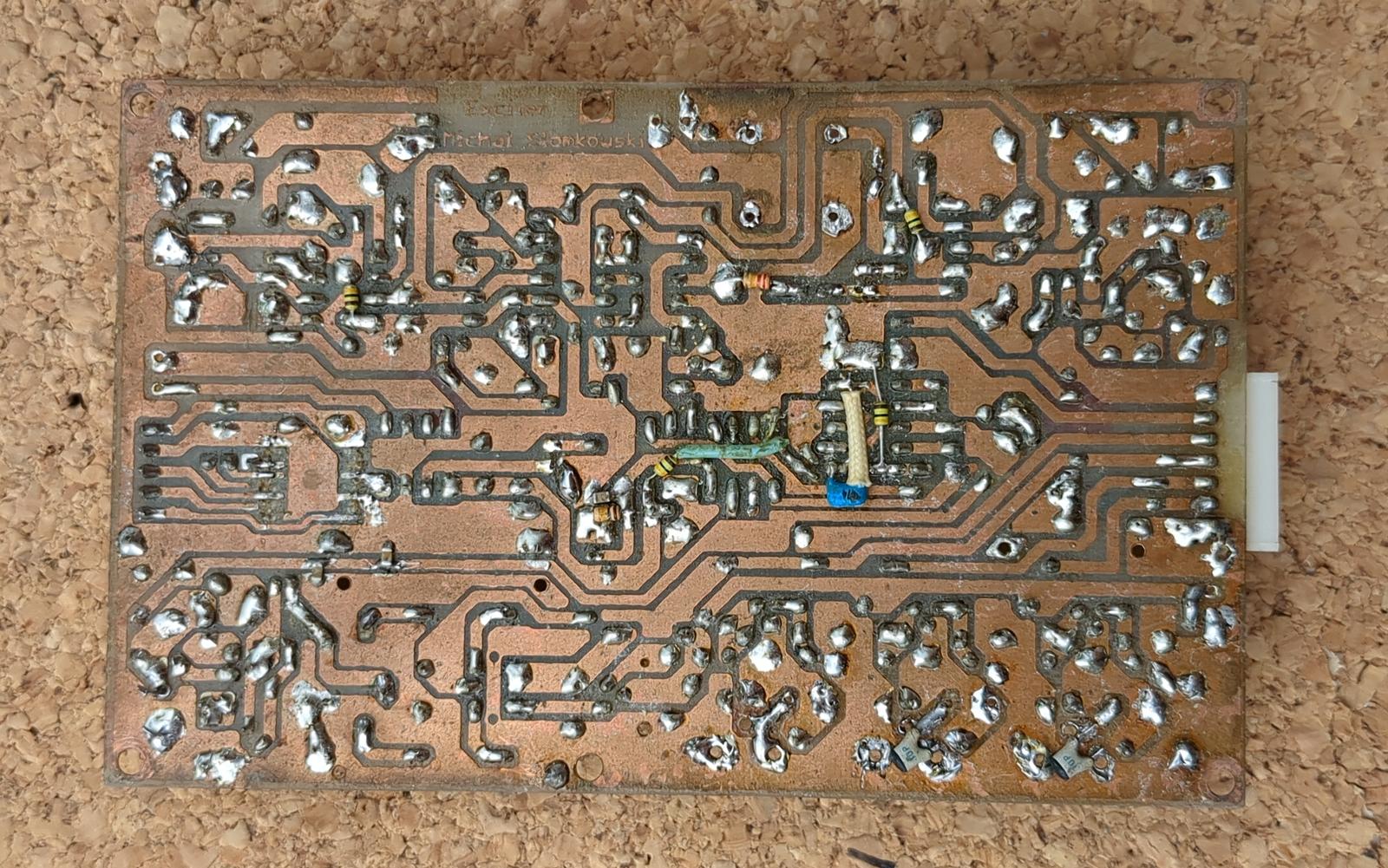
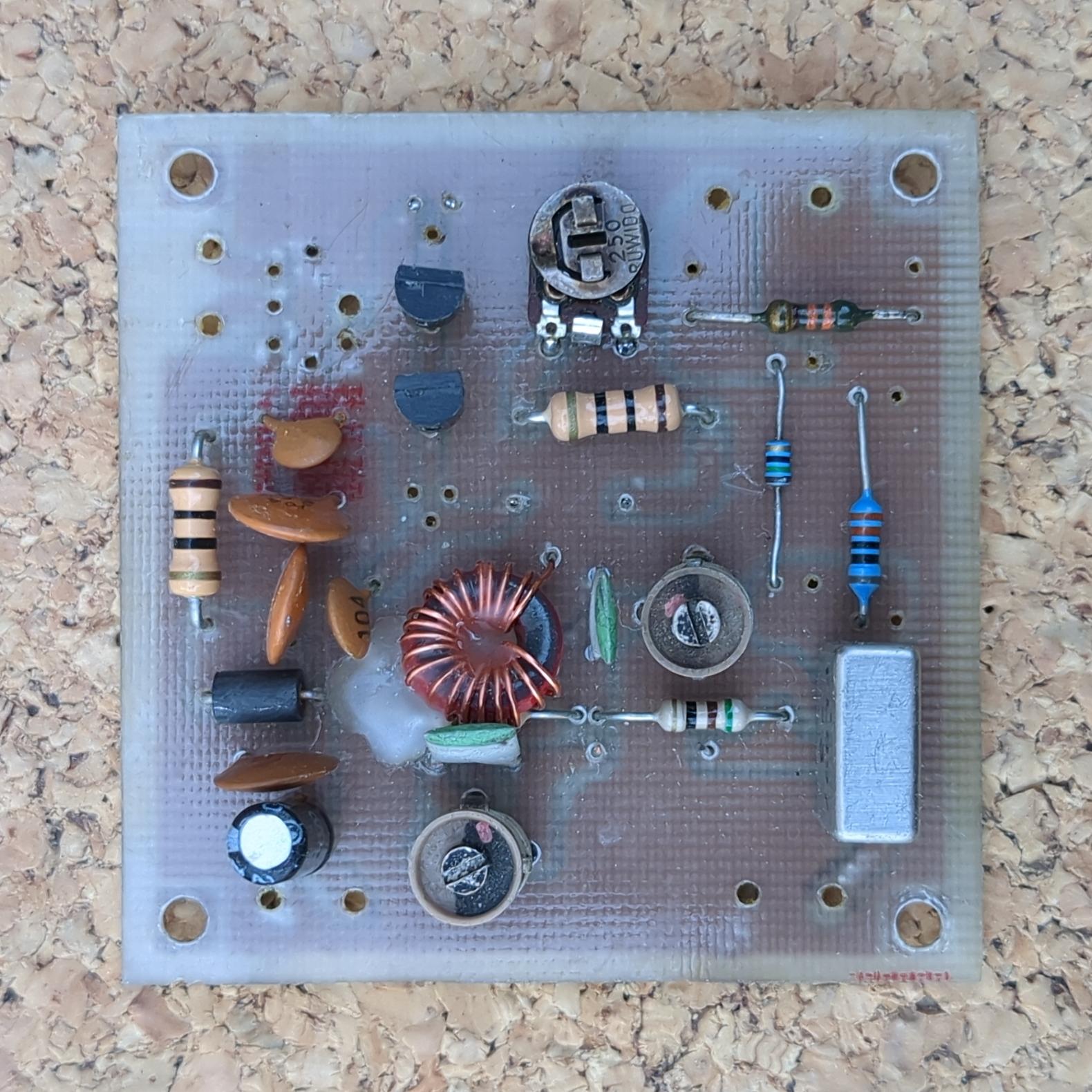
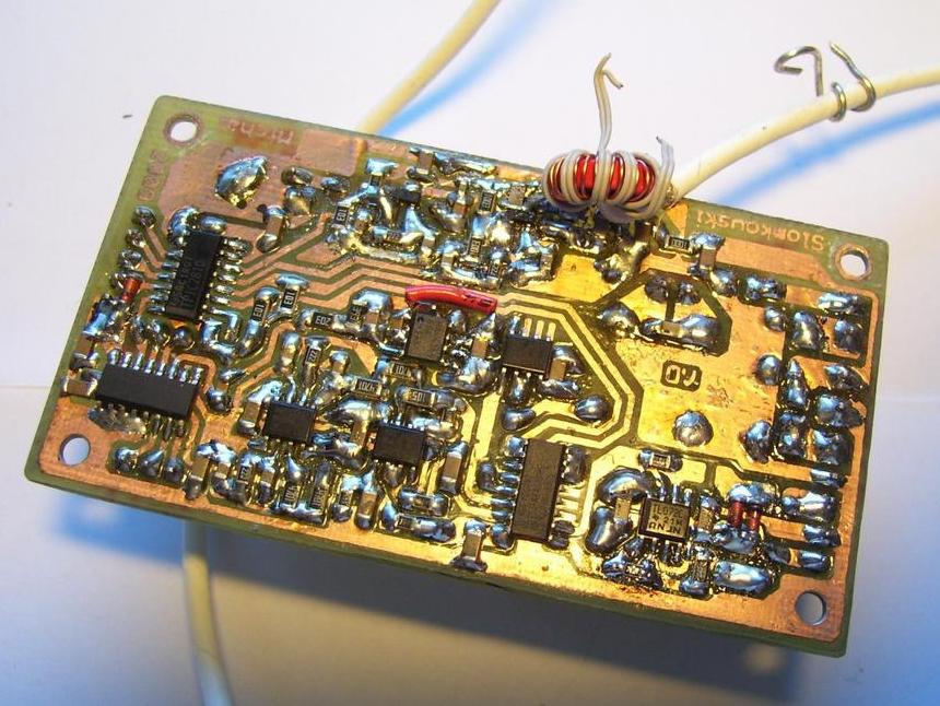
Intermediate-frequency amplifier board
Happy that I had a working VFO, I started looking for a suitable IF amplifier. Very fortunately for me, SP2JFF gave me a 9 MHz SSB quartz filter, PP9-A2, complete with a set of three resonators for the BFO oscillators. Many thanks for that! PP9-A2 is a Polish equivalent of the XF-9B from KVG. It was manufactured by OMIG, a rare example of something commercially produced specifically for amateur radio during the communist era.
SP2JFF also pointed me to the schematic of a supposedly excellent IF amplifier leveraging dual-gate MOSFETs, published in the influential Polish book Poradnik Ultrakrótkofalowca by SP6LB. In 2026, I discovered that this schematic was in fact taken from the article A Universal MOSFET IF Amplifier by Georges Ricaud, F6CER, published in QST 8/1981. I found the exact issue in PDF format, so I won’t describe the circuit in detail myself.

The board was designed in Eagle as a single-sided PCB. At the front, there is space for two
quartz filters: one PP9-A2 and a second, two-crystal ladder filter with a wider bandwidth. I’m not sure why I put it there; I probably intended to receive
AM broadcasts. The MOSFETs I used were BF964, biased with green LEDs. The IF filters F1–F5 are so-called
7x7 radio filters manufactured by the Polish company Polfer in the 1980s.
Ultimately, the board never ran successfully within the receiver. I had major problems with instability and oscillation. Probably not because of the design itself, but because of my lack of experience with RF circuits. I suspected that the IF coils were the cause of the problems, as they could couple to one another and cause the contraption to oscillate. I therefore later decided to design a new board with toroidal coils, leveraging T37-2 cores from Amidon.
Audio processing board
This PCB contained three BFO oscillators (LSB, USB, and CW), a two-diode demodulator, op-amp audio filters, and an output amplifier. At the time, I was still scared of SMD components. The schematic was lost in the abyss of the past.
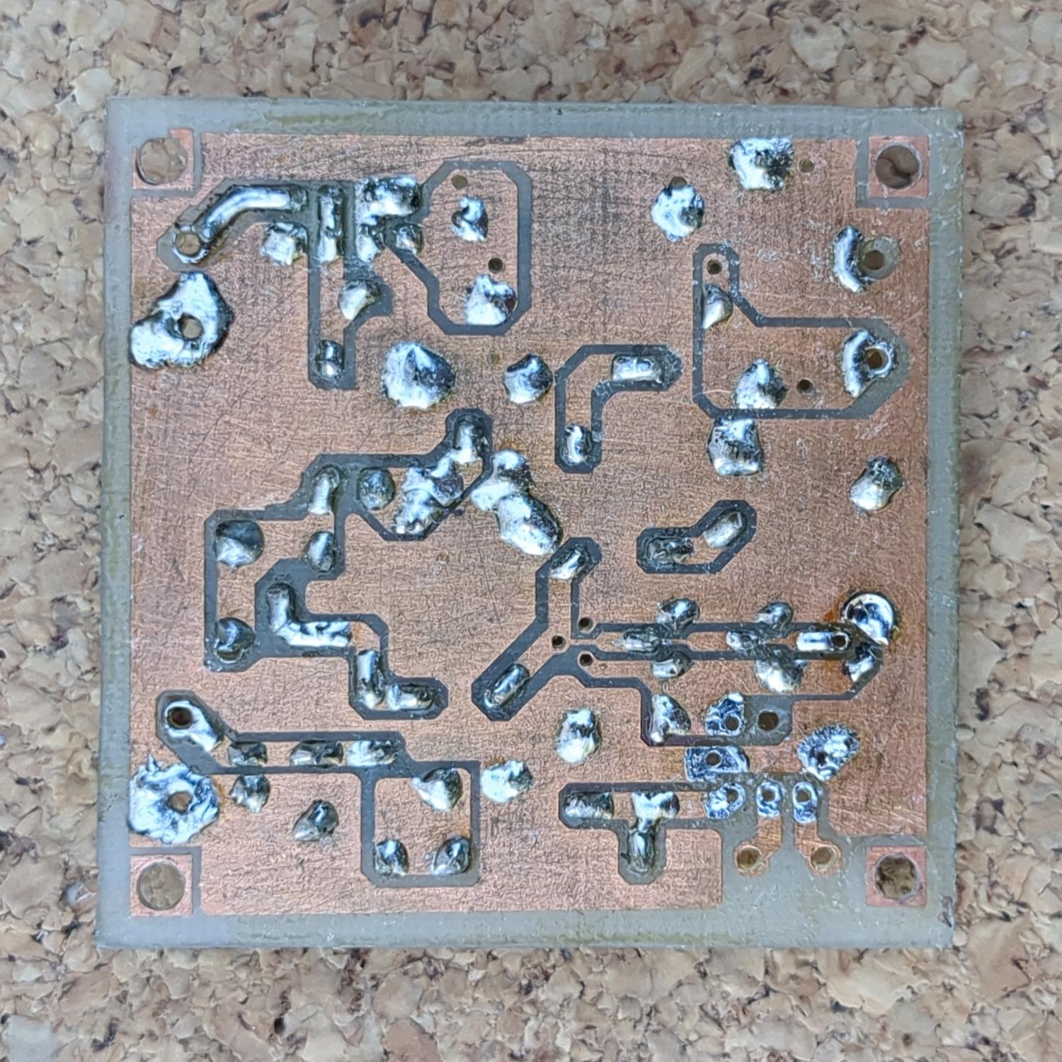
RF front end with diode mixer
This module contains a SAM3 double-balanced diode mixer with an accompanying matching circuit leveraging several BF256 FETs.

I found that board in the junk box, but I don’t remember much about it. Why was it built at all? At the time, I would have been more likely to use an AD831 as a mixer. Quite a mystery.
Attempt at IQ SDR transceiver
Frustrated with the intricacies of RF design and an IF board that turned out to be a failure, I shifted my attention to the world of software. It had already begun creeping into radio design: software-defined radio solutions with quadrature mixers such as the Tayloe mixer were becoming popular at the time. Software allowed most processing to move onto the PC and, more importantly, enabled rapid changes in the system. An SDR still requires an RF front end, but even that could be built without specialized RF components: people successfully used 74HC4053 multiplexers and PC sound cards.
I remember completing the receiving part of the planned transceiver: the VFO and the mixer board. I was not pleased with the results, though. Sensitivity was low, and I could not hear anything substantial except local stations on the 80 m band. I abandoned the project afterward but repurposed the DDS VFO board in the second attempt at a classic heterodyne transceiver. In hindsight, the failure was likely caused by the weak random-wire antenna (only several meters long). If I were to start again, I would likely build a Mini-Whip or another E-field antenna. Another factor was the poor quality of the sound card: I used a 2003 desktop PC with an integrated AC97 audio interface and did not want to invest in an external USB sound card without being sure I get better results.
DDS quadrature VFO and AVR board
To achieve an IQ baseband signal in the mixer, a VFO must provide quadrature outputs (two signals shifted by 90 degrees). I could have reused the existing AD9852 VFO board, but it had only a single output channel; generating quadrature signals would have required frequency division by four. That would have severely limited the tuning range of the receiver.
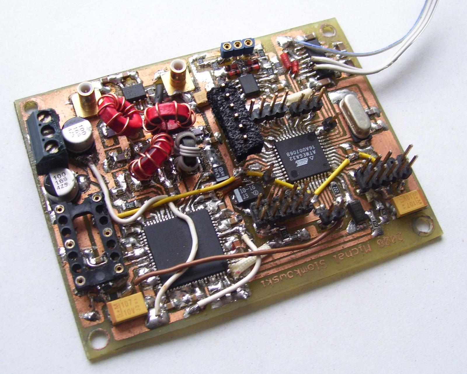
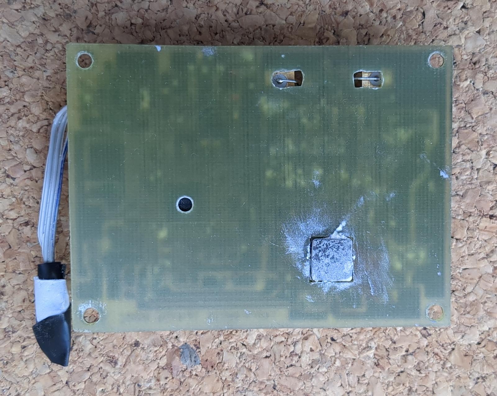
For this reason, I designed another PCB based on AD9854, a beefer DDS that sports quadrature outputs. The DDS generates two
sine waves that, after low-pass filtering, are routed to FIN1028. This chip converts the differential sine waves into LVTTL-level
square waves suitable for driving a Tayloe mixer. The quadrature LO is available on two SMB connectors named SMA1 and SMA2, which
then connect to the mixer board.
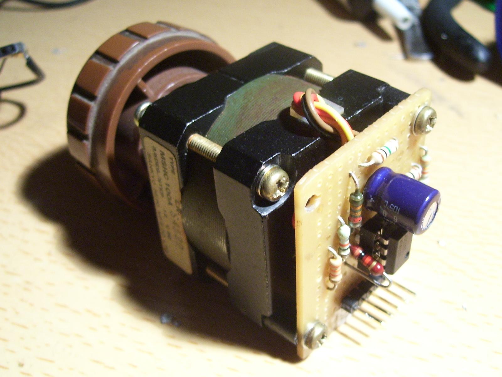
The DDS is controlled by an ATMega32 microcontroller, which also drives the HD44780-compatible LCD, tuning encoder, and facilitates communication over the RS232. A four-phase stepper motor of unknown origin was repurposed as a rotary encoder. This produced a very robust tuning dial, albeit a little quirky. I never fully implemented proper rotary encoder handling until later, during development of the Octoglow device.

As usual, the board was designed in Eagle as a single-sided PCB with many jumpers where traces crossed. I knew I pushed single-sided layout to its limits, but I was still a bit scared of double-sided PCBs. The microcontroller firmware was written in C; it did not survive. But it was just a sketch of quickly-put-together pieces of DDS, LCD and encoder procedures, nothing more.
Quadrature mixer
I wanted my transceiver/receiver to be high performance, therefore I skipped experimenting with basic 4053 mixers and moved directly to faster multiplexers. In retrospect, I should have assembled some cheap SDR kit beforehand to familiarize myself with SDR-s and have a point of reference to iterate from. No surviving photos of the board remain, but the Eagle project was still present in my archive.
At the RF input X1, there is a Mini-Circuits TT1-6, a 50 Ω wideband transformer with a bandwidth from 4 kHz to 300
MHz. The balanced signal is routed to a pair of fast demultiplexers, namely FST3253, one for receive and one for transmit.

The multiplexers are driven by quadrature LO signals from the DDS board, implementing a
Tayloe mixer configuration. The quadrature baseband signals are then amplified by instrumentation amplifiers SSM2019. Two levels
of gain are available; relay K1 selects the appropriate resistors. The amplified signal is then sent to the PC sound card (line input).
IC5A and IC5B implement integrator/low-pass filters to compensate DC offset. The audio output is averaged over time, and the
resulting voltage is used as a bias for the instrumentation amplifiers. DC offset
happens often in SDR circuits, and there are various ways to fight it.
The transmit quadrature signal from the sound card output is amplified by a pair of TL072D and mixed with the LO in
IC2. Unfortunately, this section was never tested, as the project was abandoned after the receiver performance proved poor.
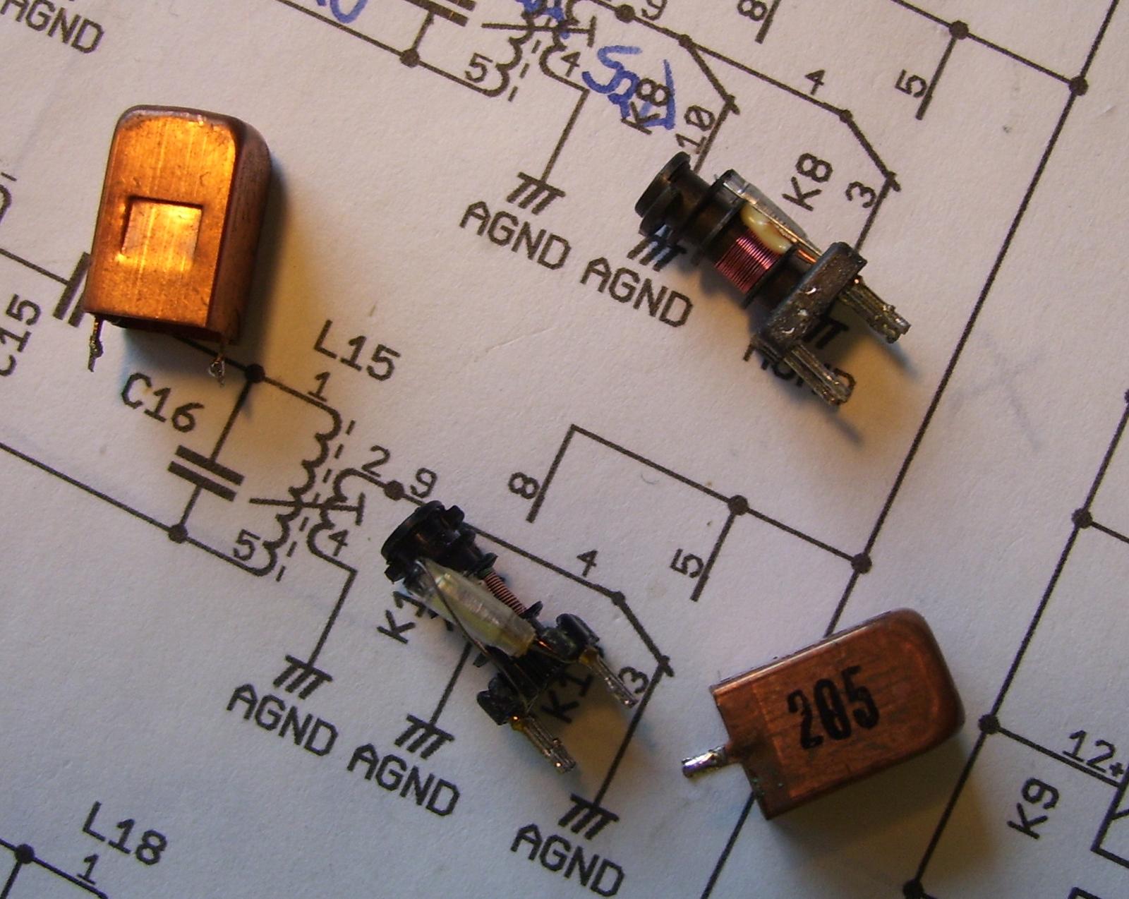
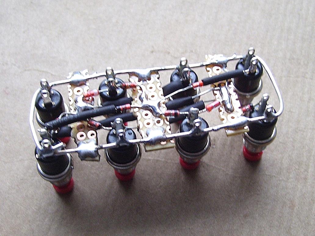
Bandpass filters
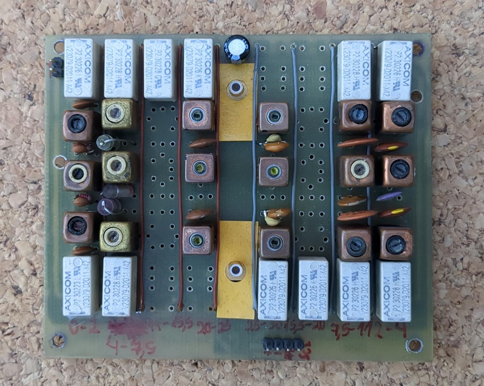
The SDR bandpass filters were intended not only for amateur bands but for the full 0–30 MHz range, divided into eight segments. Their design was inspired by an amateur receiver called DigiReX. This was an interesting albeit low-performance receiver for HF, which performed DSP on the AVR microcontroller! More details available on its archived website and forum thread.

The filters are switched to the SMB connectors by miniature relays. The relays are driven by TPIC2810, an 8-channel driver with I2C interface. The coils were made from carcasses extracted from Polfer 7x7 radio filters, mentioned earlier. Some coils were of different origin. Only six filters were completed; I tuned them using an oscilloscope, a dummy load, and the DDS synthesizer described above. The coils were wound by hand and placed in the original brass shields before being soldered to the PCB. I’m not sure, but I probably calculated the required number of turns of my coils by counting the turns on the original coils and comparing the desired inductance with the datasheet. I didn’t measure the actual inductance because I didn’t own an inductance meter at the time.
Another attempt at 9 MHz heterodyne transceiver
As I was shelving the SDR project, I noticed the PP9-A2 crystal filter lying dormant, prompting me to do something with it. I already had some modules more or less ready: the quadrature VFO and the input filter board. So I returned to the classic heterodyne, but this time I was going to use dedicated ICs and build a transceiver, or at least make the design extendable to include transmission capability later. The planned specification was as follows:
- full coverage 0.1 – 30 MHz
- first mixer chip AD831 — theoretical IP3 at +24 dBm
- intermediate frequency — 9 MHz, OMIG PP9/A2 quartz filter used — a Polish version of the well-known KVG XF9B
- IF amplifier — MC1350, product detector — MC1496
- VFO on the AD9854 DDS
- control board powered by an ATMega32 microcontroller
- VFO dial encoder made from a stepper motor
- galvanic isolation for audio output and USB port
- output power: unknown yet
Only a small part of this specification came to fruition, though. In fact, it could be summed up as an SSB receiver on the 160, 80, and 40 m amateur bands with a digital VFO and manual gain control. Again, a failure, but one with a lot of experience gained.
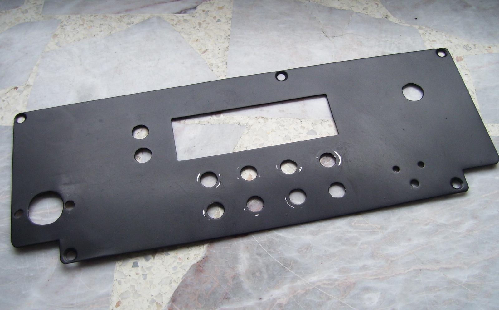
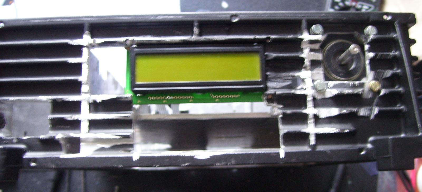
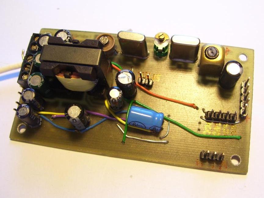
As for the cabinet, I repurposed an aluminum extruded case that previously housed some RF equipment, probably an analog NMT cellphone. Several holes were cut into it in an ugly manner, and a piece of steel plate acted as a crude front panel. On the back, there were a 230 V power supply socket, a USB port, and a standard UC-1 connector for the antenna.
The power supply was a classic one (transformer, rectifiers, and 78xx/79xx regulators). It provided +12 V, +10 V, and -12 V. Some shielding was used inside, but I don’t think it made any difference. SMB cables, salvaged from the aforementioned NMT cellphone, connected the RF boards within the device.
The front panel featured a 2x16 LCD, eight buttons, and a VFO dial described in the previous section. The firmware wasn’t backed up and didn’t survive (I had yet to learn to use version control at that time). Several years later, during a cleanup, I disassembled it, threw away the chassis, and put the PCBs in the failed projects box.
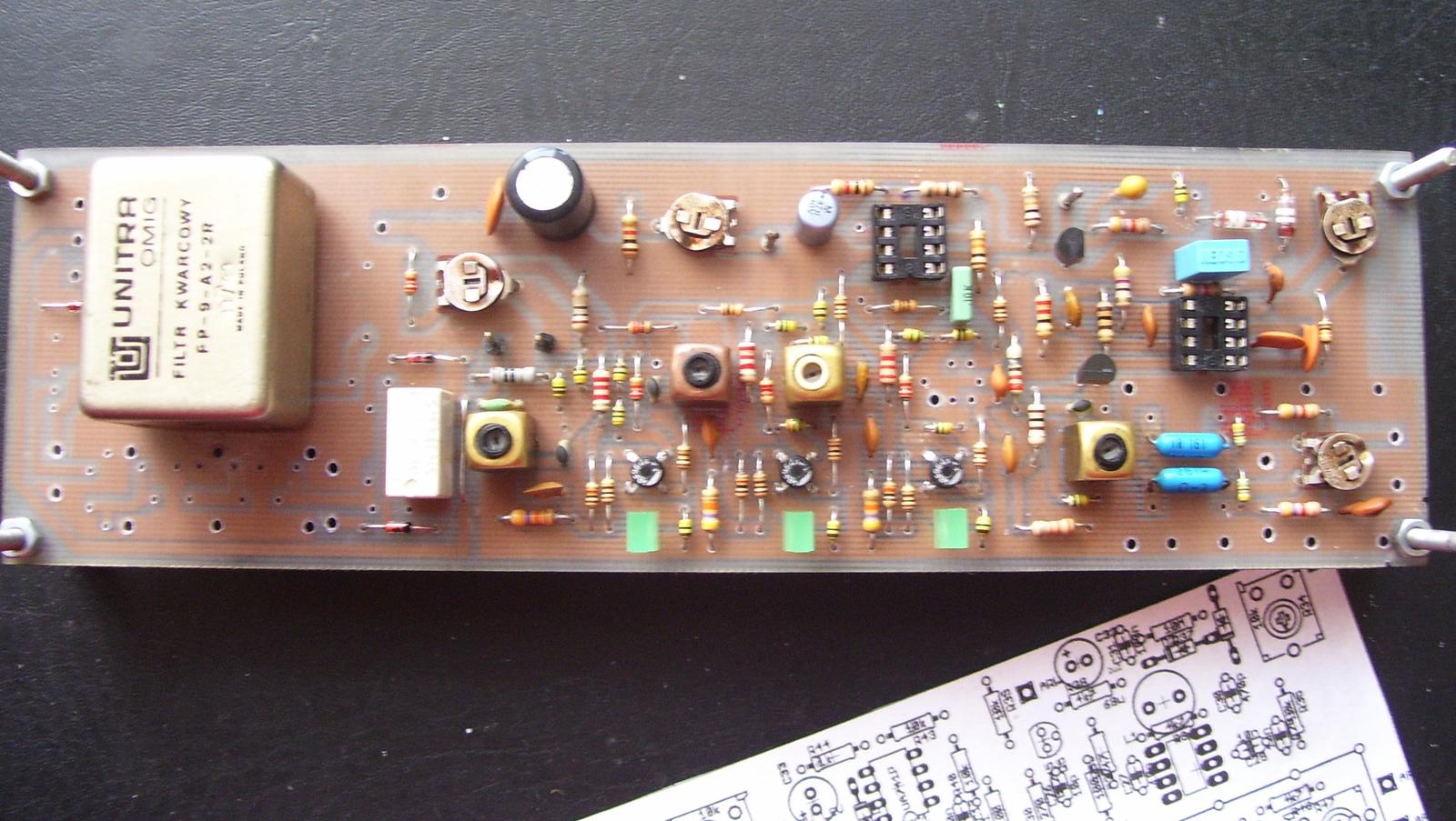
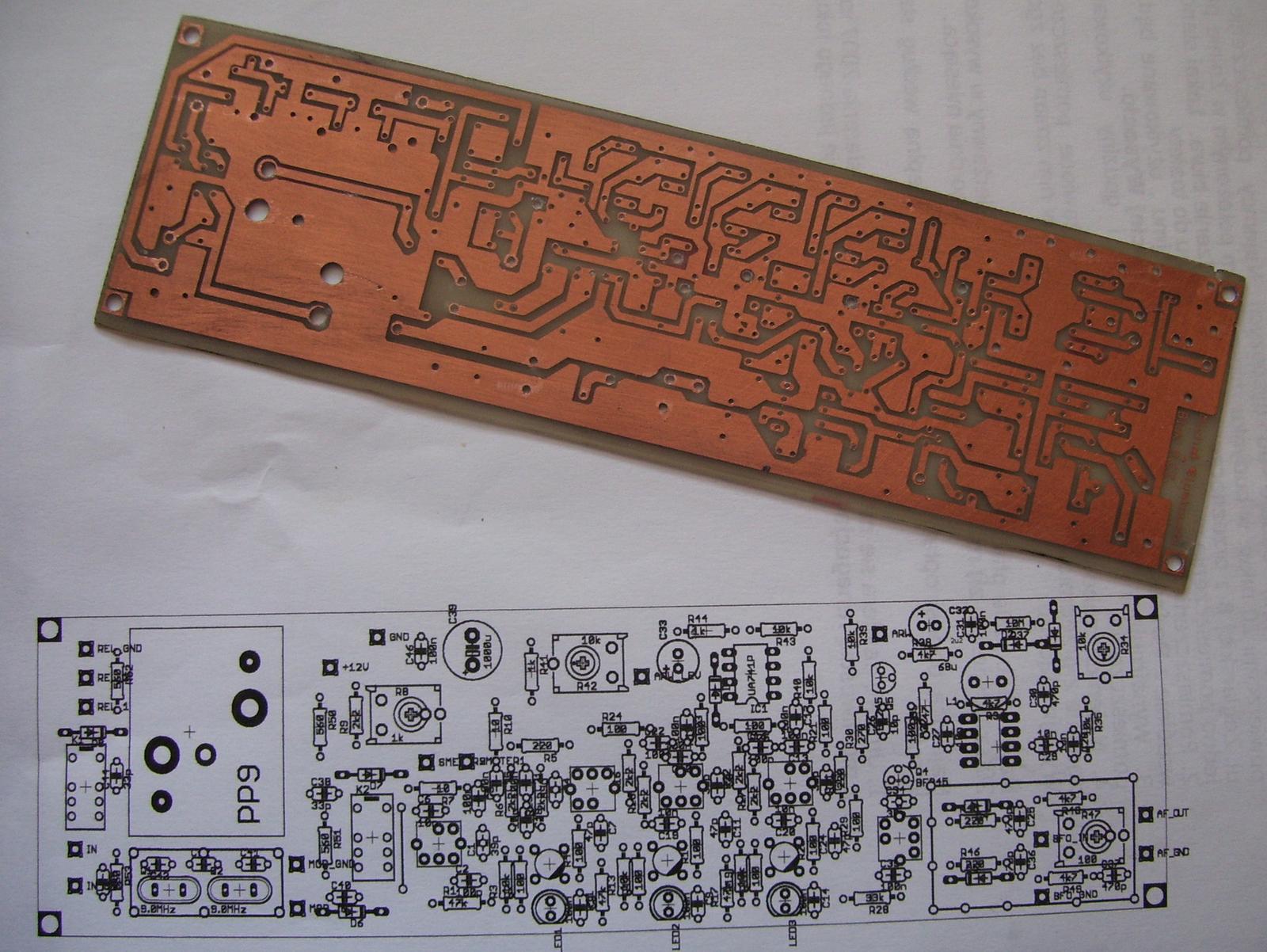
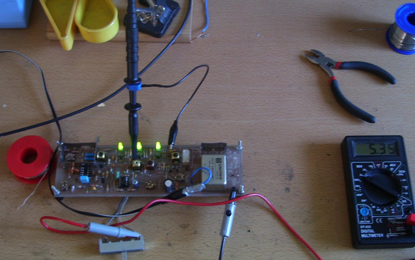
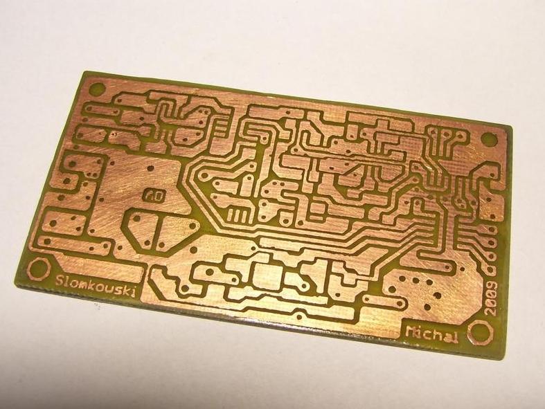
Radio-frequency board
In my second attempt at a classic heterodyne, I leveraged more integrated circuits than before. I tried to avoid discrete components, since they are more problematic. The PCB (Eagle files) is double-layer for the first time, although the top copper layer is just a ground plane. The power is the usual +12 V, but the mixer is supplied from a separate +10 V line.
The signal path starts at the RF_IN SMB connector and is routed to the Mini-Circuits TT1-6 wideband
transformer, which converts the unbalanced signal to a balanced one for the AD831 mixer inputs. This IC is very nice: it works
from DC up to 500 MHz, the LO signal can be a sine or square wave, and its input and output impedance can be easily controlled. The IP3 parameter is +24 dBm, which is sufficiently high — much higher than
that of the widely used NE602. The PLCC package, despite being SMD, is big enough to be easily soldered. Its disadvantage is high
current consumption; it could be lowered, but the IP3 would suffer.

After the mixer, there are two quartz filters, selectable by a diode switch realized on PIN diodes
D1–D8. The first quartz filter is the aforementioned PP9-A2; the place for the other filter is not populated. I had an empty
metal case for a crystal filter at hand and planned to make a CW filter from discrete 9 MHz quartz resonators.
The IF amplification is done by the well-known MC1350 amplifiers. Each amplifier is coupled to the next stage by a resonant
transformer wound on a T37-2 core. I don’t have the calculations or the number of turns on the coils, though. Toroidal cores have
a great advantage over factory-made open IF coils: they don’t leak as much magnetic field, so they don’t couple with each other and don’t cause
instabilities. The IF signal is once again filtered by a two-quartz ladder filter, Q1–Q2, and demodulated by the MC1496, also used in the SSB exciter. The BFO signal is provided by an oscillator on the
audio board.
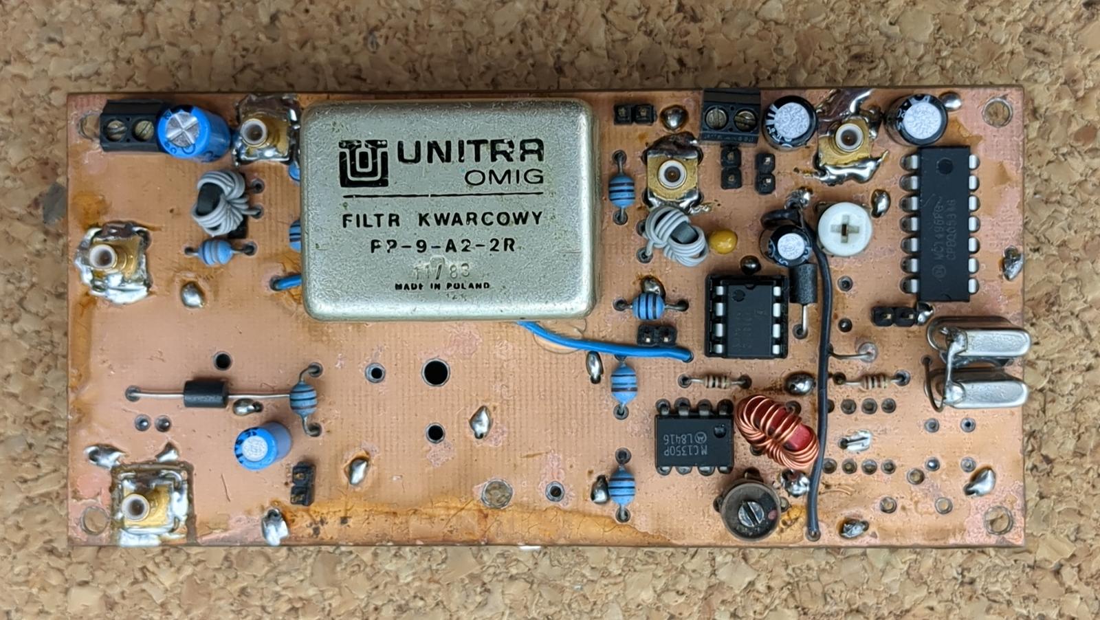
The MC1350’s REG inputs are for controlling the gain, leveraged by the automatic
gain control. The IF signal after the second amplifier is rectified, smoothed in RC filters, and amplified in a CA3130 op-amp.
I remember I took this circuit from somewhere, but I don’t remember from where. This is the weakest part of the receiver. I couldn’t get it to work
properly. I tried some other circuit (hence the universal PCB), but the problems prevailed. Finally, I switched to manual gain regulation via a separate
potentiometer on the front panel, to have it working at least partially.
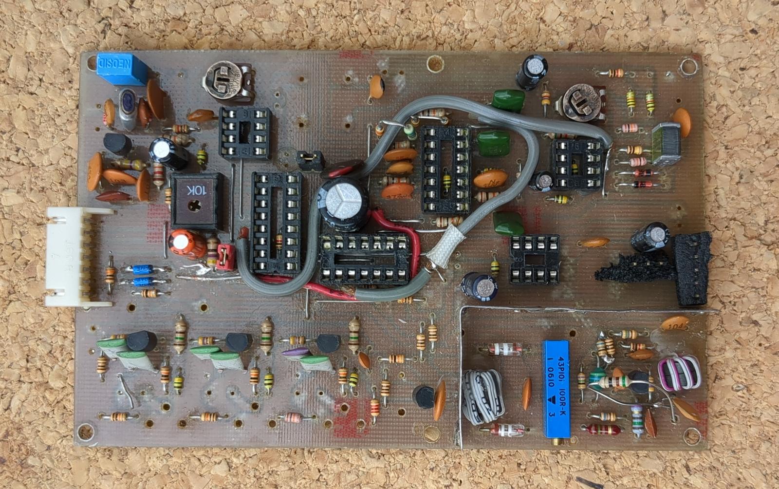
Audio and BFO board
This section was originally published in 2009 on my old website, flylab.ovh.org. The text was redacted, but the general structure was kept intact.
The schematic was created at a fairly advanced stage of the project, so I managed to avoid many mistakes I had made in previous modules. Because my experience in making printed circuit boards had increased much since then, the board (Eagle project) looks quite good. The up-to-date schematic differs a bit from the version presented in the photos (mainly the BFO block). See them below:
The supply voltages needed are +12 V and -12 V, +5 V for the analog part, and +5 V for the digital part. You can use one 5 V power supply instead of two separate ones, but this might increase the level of noise from the digital part.

The signal from the product detector is delivered to the input AF_IN1 or AF_IN2. Diode limiters protect the inputs and muffle
the clicks and pops somewhat, so they are not so annoying. The operational amplifiers IC1A and IC1B amplify the signal to the
level needed to drive the audio power amplifier, and also make it possible to have equal levels from both inputs. This is done by changing the values of
the feedback resistors (R2 and R4). With acceptable noise, up to 40 dB of signal amplification can be achieved.
The values in the schematic are adjusted to my specific case (it depends on the product detector and speaker).
From the many operational amplifiers available, I chose the very popular TL072. They are quite low-noise and very cheap.
Because of the large gain in the circuit, the noise might be a little too high, so you may use an NE5532 as IC1
instead of the TL072. Unfortunately, I had some problems when I tried to get them in an SMD package. One of the modern ultra-low-noise amplifiers, e.g.
from Analog Devices, would be even better.
I put two inputs on the circuit because I had been planning to make an additional receiver block through which I could listen to VHF bands. It could be any other source that produces baseband audio, for example a classic diode detector to listen to AM stations in much better quality.
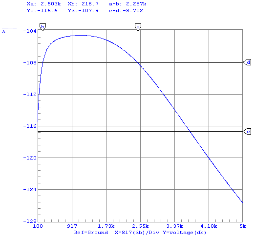
Then, the signal comes through the analog multiplexer IC2 (4053) to the group of high- and lowpass active filters,
implemented on the IC3A, IC4A, and IC4B op-amps. They filter the audio signal to eliminate out-of-band noise and
distortion. The frequency response was calculated using the SPICE circuit simulator and is shown in the figure below. The band’s half-power points are 200
Hz and 2.5 kHz. This makes the filter suitable for human speech.
The filtered signal goes to the digital potentiometer DS1881, which is used to change the audio volume. The maximal attenuation is approximately 60 dB. Then, the signal is delivered to the input of the audio power amplifier MAX4364, which drives the speaker or headphones.
Instead of the well-known but also heavily criticized LM386, I used a quite unpopular alternative — the MAX4364. It can deliver up to 1.4 W into an 8 Ω load. I got it from the sample program from Dallas-Maxim. A slightly extraordinary concept is the volume regulation by the digital potentiometer. It gives me the possibility of controlling it with the microcontroller, and then remotely from a computer. There’s one inconvenience, though: one knob has two functions, VFO and volume (switchable by a button).
In addition, there’s a buffer IC5B and an audio frequency transformer TR1. It separates the audio output from the
transceiver’s core circuits. This is necessary for a safe connection between the radio and the computer. The signal is taken from either the input or the
output of the active filters, switchable by the multiplexer IC2.
The carrier wave generator (BFO — beat frequency oscillator) is based on a slightly modified Colpitts oscillator. It is present in two copies, for the
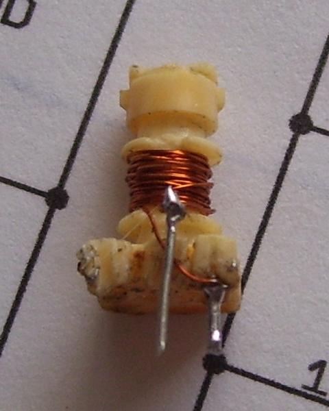
upper and lower sideband respectively. Switching is done by the I2C driver TPIC2810. The coil in the collector’s
resonant circuit has 26 turns of 0.3 mm magnet wire (AWG 28) wound on a T37-2 toroid core (AL = 4). This gives 2.7 μH of inductance. The output signal is
tapped from an additional winding on the L2 coil. One turn gives approximately 140 mV effective voltage into a 50 Ω load (-4 dBm). It’s enough
to properly drive modern IC double-balanced mixers, such as the NE612, MC1496, or AD831. If you use a classic diode mixer, a higher signal level is required (usually 7 or 13 dBm).
The coil connected to one of the resonators is wound on a core from an FM intermediate frequency filter. The required inductance is in the range of 5 – 10 μH, depending on the quartz resonator. I used a Polish 7x7 filter, but I think they are similar to any others produced in Japan or China. I wound 25 turns of 0.2 mm enameled copper wire (AWG 32).
Originally, there was no resonant circuit, only a 1 kΩ resistor. Unfortunately, the shape of the output signal was very distorted, despite the reduction of the feedback capacitance. To make the signal cleaner, I added the LC circuit. The 1 kΩ resistor is necessary, otherwise the generator probably won’t oscillate. Unfortunately, this change altered the connections a little, so I had to place the coil on the copper side.
I used standard 9.000 MHz quartz resonators. A coil or capacitor is placed in series with the resonator to shift its resonant frequency 1.5 kHz up or down. For differential mixing (VFO frequency greater than the intermediate one), the BFO should generate 9001.5 kHz for the upper sideband and 8998.5 kHz for the lower one. It’s possible, or even better, to use the original resonators provided with a quartz filter. Then, for fine-tuning, you should use a 30 pF variable trimmer in parallel with a 22 pF capacitor for both resonators. Using a frequency counter, tune the generator at the target load. You should also consider stabilizing the collector filter coil mechanically, since changing its inductance affects the BFO and its frequency.
If you don’t have a frequency counter, there’s a way to align the BFO without one. Unfortunately, you also need a completed and working receiver block and VFO. Tune to a strong AM station so that the VFO frequency is lower or higher by 1.5 kHz (depending on the sideband), then trim the capacitor or coil until the carrier tone disappears.
The control of the module is implemented using I2C. The TPIC2810 (IC8) is an 8-channel driver with
open-collector (drain) outputs. It’s available for writing at the address 0x60. To understand how it works, it is recommended to read its
datasheet. The IC switches on the proper BFO oscillator and controls the 4053 multiplexer. Unused outputs are available on the connector OC.
The diode was connected to the pin DRAIN7 because that pin used to drive the external relay.
The second I2C device is a dual-channel digital logarithmic potentiometer, the DS1881. It allows setting the volume
in 32 or 64 steps, with a maximal attenuation of 60 dB. Its unused channel is available on the socket named POT.
The assembly process is typical for SMD components. A large number of jumpers may be stressful and could drive you nuts. I had to use them because I
still couldn’t produce double-sided PCBs. The resistor R27 is an exception: you have to solder it on top of the C5 capacitor.
That inconvenience was caused by a design error; I had forgotten about this resistor in the original design. It’s better to solder the L2 coil
on the copper side, since there’s more room there.
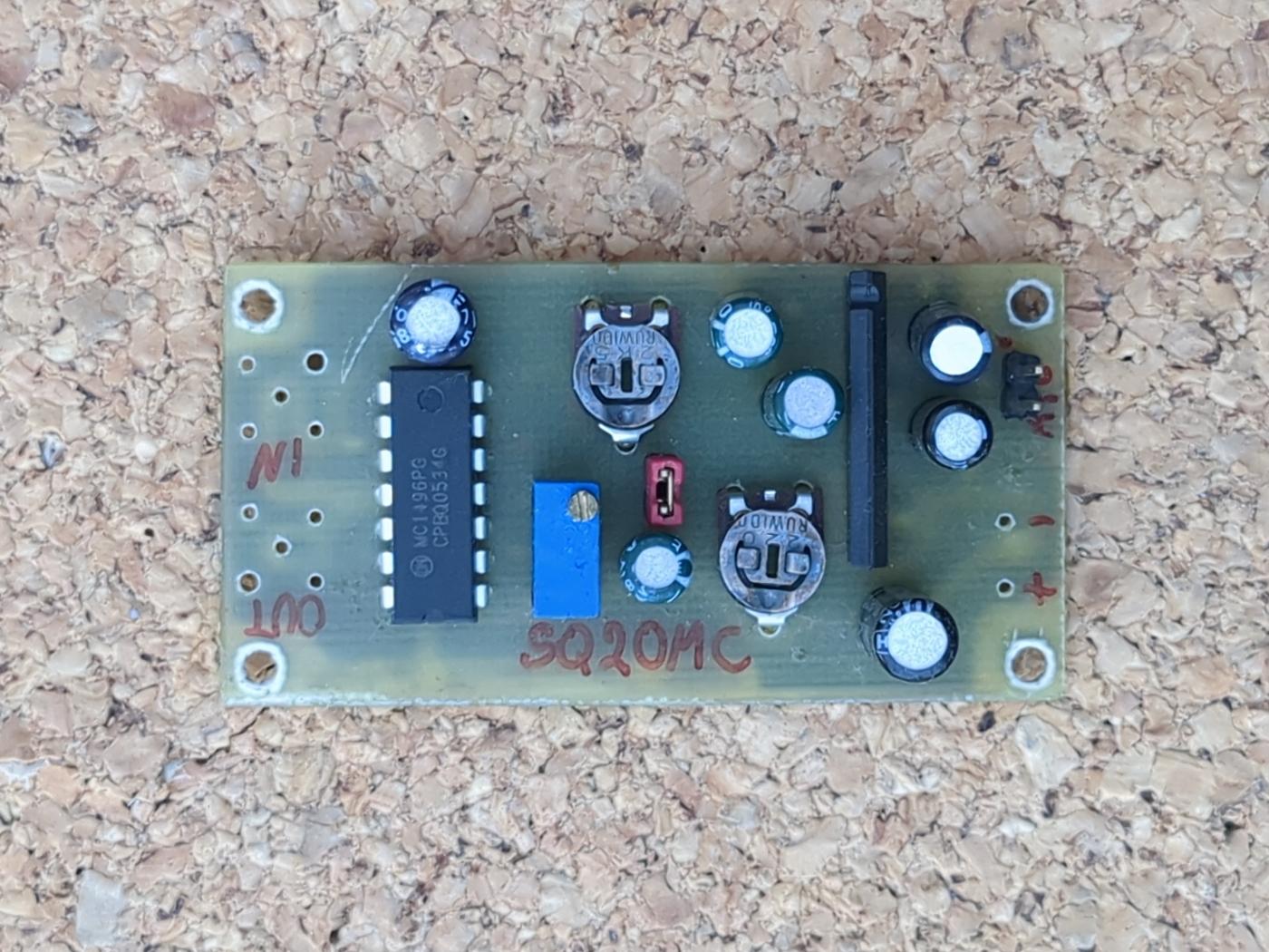
SSB exciter
Based on the application notes of the balanced modulator/demodulator MC1496 and the audio amplifier BA3308.

I think I didn’t even run this board at all. It is probably supposed to work with a dynamic microphone and
generate a DSB signal, which would be routed to the TX_IN connector on the RF board.
Lessons learned
Phew, that was quite a trip down memory lane! A lot of boards produced and a lot of learning done. Despite the failure, my electronics skills increased tremendously.
What should I have done differently? The project failed largely because of perfectionism: instead of getting some minimal viable product, I kept redesigning. I had almost no measuring equipment — affordable devices like the NanoVNA simply did not exist yet, and professional VNAs and spectrum analyzers were far beyond my reach.
A much better starting point would have been a simple single-band SSB transceiver, a proven design popular in Poland at the time, such as Antek.
Besides, building a proper antenna for the 80, 40, and 20 m bands before diving into the receiver would have saved a lot of frustration. It would have provided instant feedback during development and spared me the trips to the ham club.
In my reboot of the amateur radio hobby, in order not to lose myself in arcane microwave sciences, I simply bought a Pluto+ SDR, and now I’m working on a setup for the QO-100 satellite.